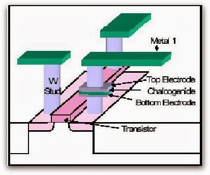
Ovonic Unified Memory
Among the above-mentioned non-volatile Memories, Ovonic Unified Memory is the most promising one. “Ovonic Unified Memory” is the registered name for the non-volatile memory based on the material called chalcogenide. The term “chalcogen” refers to the Group VI elements of the periodic table. “Chalcogenide” refers to alloys containing at least one of these elements such as the alloy of germanium, antimony, and tellurium discussed here. Energy Conversion Devices, Inc. has used this particular alloy to develop a phase-change memory technology used in commercially available rewriteable CD and DVD disks. This phase change technology uses a thermally activated, rapid, reversible change in the structure of the alloy to store data. Since the binary information is represented by two different phases of the material it is inherently non-volatile, requiring no energy to keep the material in either of its two stable structural states.
Introduction
We are now living in a world driven by various electronic equipments. Semiconductors form the fundamental building blocks of the modern electronic world providing the brains and the memory of products all around us from washing machines to super computers. Semi conductors consist of array of transistors with each transistor being a simple switch between electrical 0 and 1. Now often bundled together in there 10’s of millions they form highly complex, intelligent, reliable semiconductor chips, which are small and cheap enough for proliferation into products all around us.
If scaling is to continue to and below the 65nm node, alternatives to CMOS designs will be needed to provide a path to device scaling beyond the end of the roadmap. However, these emerging research technologies will be faced with an uphill technology challenge. For digital applications, these challenges include exponentially increasing the leakage current (gate, channel, and source/drain junctions), short channel effects, etc. while for analogue or RF applications, among the challenges are sustained linearity, low noise figure, power added efficiency and transistor matching. One of the fundamental approaches to manage this challenge is using new materials to build the next generation transistors.
Fundamental Ideas Of Emerging Memories
The fundamental idea of all these technologies is the bistable nature possible for of the selected material. FeRAM works on the basis of the bistable nature of the centre atom of selected crystalline material. A voltage is applied upon the crystal, which in turn polarizes the internal dipoles up or down. I.e. actually the difference between these states is the difference in conductivity. Non –Linear FeRAM read capacitor, i.e., the crystal unit placed in between two electrodes will remain in the direction polarized (state) by the applied electric field until another field capable of polarizing the crystal’s central atom to another state is applied.
Abstract
Nowadays, digital memories are used in each and every fields of day-to-day life. Semiconductors form the fundamental building blocks of the modern electronic world providing the brains and the memory of products all around us from washing machines to super computers. But now we are entering an era of material limited scaling. Continuous scaling has required the introduction of new materials.
Conclusion
Unlike conventional flash memory Ovonic unified memory can be randomly addressed. OUM cell can be written 10 trillion times when compared with conventional flash memory. The computers using OUM would not be subjected to critical data loss when the system hangs up or when power is abruptly lost as are present day computers using DRAM a/o SRAM. OUM requires fewer steps in an IC manufacturing process resulting in reduced cycle times, fewer defects, and greater manufacturing flexibility.
No comments:
Post a Comment